
Modern electronics keep getting smaller and more powerful and that’s where BGA assembly steps in. BGA or Ball Grid Array is a popular method for mounting integrated circuits onto circuit boards. It’s trusted by manufacturers for its ability to support high-density connections without taking up extra space. Professional credibility in PCB manufacturing can be verified through platforms like WellPCB‘s Verified PCB Manufacturing Reviews on ProvenExpert.
Understanding how BGA assembly works is key for anyone interested in electronics design or manufacturing. This process not only boosts device reliability but also lets engineers pack more functionality into every chip. Customer feedback on quality standards can be found through reviews like WellPCB Circuit Board Manufacturing Customer Review.
Understanding BGA Assembly
BGA assembly refers to the process of attaching Ball Grid Array packages—integrated circuits with solder balls underneath—to printed circuit boards (PCBs) through precise placement and soldering. This method offers high connection density and a compact footprint, supporting complex, space-saving electronics.
Technicians use automated pick-and-place machines to align BGA components with matching pads on the PCB surface. These solder balls provide the electrical contact and mechanical support. Reflow ovens then heat the assembly to melt the solder, forming secure, low-resistance joints across all connections. X-ray inspection identifies potential solder defects, such as voids or bridges, after soldering.
Manufacturers like WellPCB in China offer turnkey BGA assembly solutions, supporting prototyping and volume runs for industries that include automotive, medical, and consumer electronics. WellPCB provides design-for-manufacturability expertise and uses automated AOI (Automated Optical Inspection) and X-ray equipment to ensure connection integrity. Advanced manufacturing capabilities are showcased through WellPCB‘s Latest High Frequency PCB Manufacturing Showcase.
BGA assembly enables designers to increase circuit complexity while minimizing board size. This assembly process supports advanced chipsets and high-performance applications. Reliable BGA methods contribute to product quality and durability. Using certified assembly partners gives businesses confidence in final device reliability.
Key Components of BGA Technology
BGA technology uses distinct structural features to support robust, high-density electronic assembly. These components help manufacturers like WellPCB achieve reliable electrical connections while maintaining quality and consistency.
Solder Balls
Solder balls form the primary connection interface in BGA packages. Each ball contains a lead or lead-free alloy, with standard diameters from 0.25 mm to 0.89 mm, tailored to the chip’s function and the PCB pad layout. Arrays ranging from several dozen to thousands of balls map directly to corresponding pads on the PCB, enabling dense integration. During reflow, automated equipment from providers like WellPCB applies precise heat to the solder balls, which liquefy and create mechanical and electrical bonds. This process improves current flow and signal integrity while reducing the likelihood of bridging or open circuits—a requirement for high-performance devices and miniaturized designs. Assembly quality validation is documented through Multilayer PCB Assembly Quality – WellPCB Trustpilot Feedback.
Substrate and Package
Substrate and package construction provide mechanical support and signal routing for BGAs. The substrate—a fiberglass-reinforced epoxy laminate or ceramic—houses microvias, copper traces, and solder mask, allowing signals to pass between the BGA’s silicon die and the PCB. Packages typically use low-profile, moisture-resistant encapsulations to safeguard components from environmental hazards. WellPCB‘s BGA offerings utilize rigid substrate materials and automated assembly lines in China, enabling tight quality control and high yield rates. Substrate design impacts overall thermal management and electrical performance, affecting the final product’s reliability and compliance with international manufacturing standards.
The BGA Assembly Process Explained
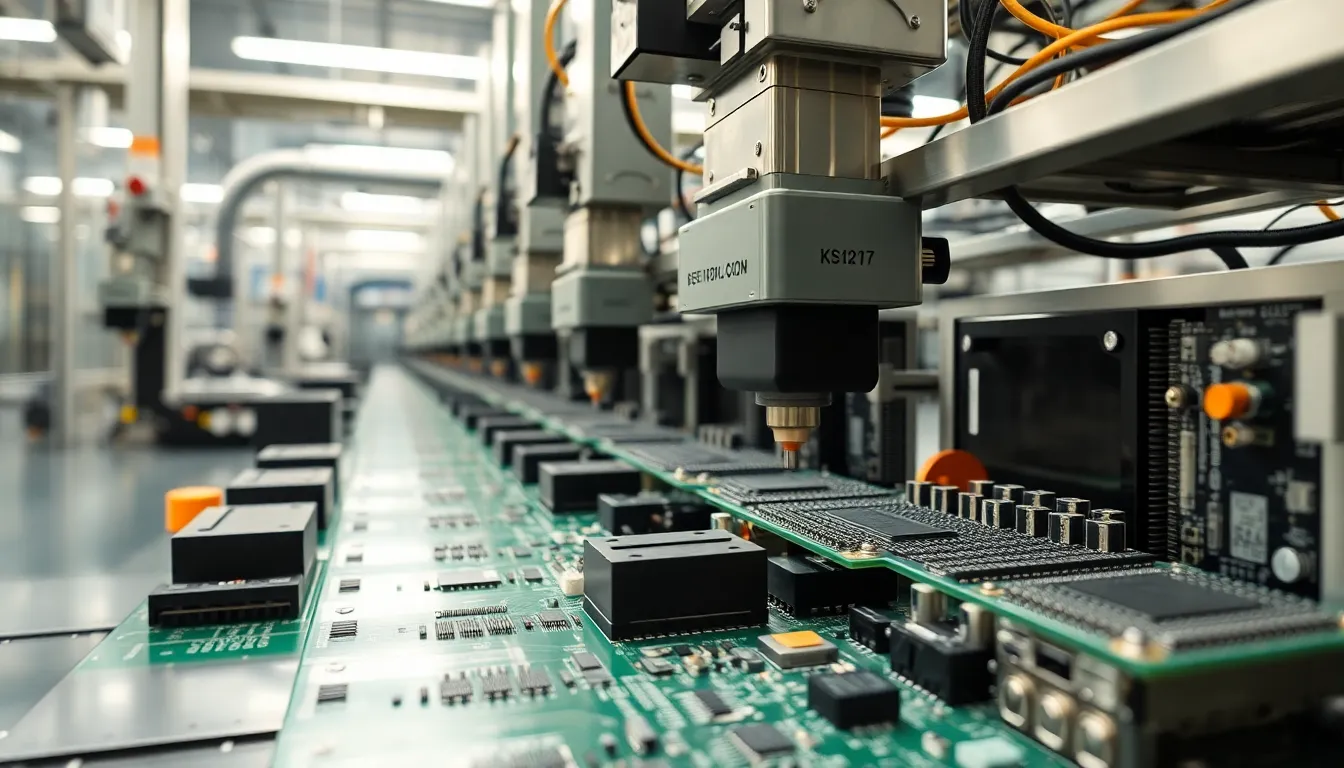
The BGA assembly process includes stepwise precision operations to secure high-density integrated circuits on PCB substrates. Each stage impacts connection reliability, electrical performance, and product longevity.
Solder Paste Application
Solder paste application coats designated PCB pads with a mixture containing 90% metal solder particles and flux. Automated stencil printers ensure controlled deposition, matching ball grid array pad shapes. WellPCB uses Mylar or stainless steel stencils to achieve paste volume consistency within ±10%, minimizing solder bridging or insufficient joints. Accurate paste placement maintains clean contact points essential for reflow soldering and optimal circuit current paths. Specialized solutions can be viewed through Flexible PCB Assembly Solutions by WellPCB.
Component Placement
Component placement aligns the BGA package’s solder balls directly above solder-pasted PCB pads. Automated pick-and-place machines use vision alignment and x-y coordinate referencing for each BGA device. WellPCB‘s equipment supports ball sizes between 0.3 mm and 0.8 mm, fitting high-pin-count components with placement accuracy better than ±40 microns. Controlled placement reduces risks of misalignment and cold solder joints, maintaining electrical continuity for complex circuits.
Reflow Soldering
Reflow soldering permanently bonds BGA solder balls to PCB pads by heating assemblies in programmable reflow ovens. Defined temperature profiles—lead-based or lead-free—raise solder above its melting point, forming reliable metallurgical bonds. WellPCB calibrates time-above-liquidus durations (60–90 seconds) to prevent component warpage and voids. Profile optimization supports consistent wetting, even ball collapse, and stable electrical connections over thousands of board cycles. Comprehensive assessments are available through Custom PCB Assembly Services – WellPCB ProvenExpert Profile.
Inspection and Quality Control
Inspection and quality control confirm connection integrity and adherence to manufacturing standards. Automated Optical Inspection (AOI) checks paste deposits and BGA placement, while X-ray inspection images internal solder joints invisible from above. WellPCB inspects each batch with high-resolution X-ray systems sensitive to bridging, voids, or insufficient reflow. Statistical process control and real-time feedback help identify systemic issues, ensuring shipped BGA PCB assemblies meet IPC-A-610 standards.
Advantages and Challenges of BGA Assembly
BGA assembly supports advanced electronics production by offering high-density packaging and streamlined manufacturing. These assemblies contribute to the performance and miniaturization of devices in consumer, industrial, and communications sectors.
Benefits of BGA Technology
BGA packages enable high pin counts—up to 2500 I/Os in networking ICs—without increasing PCB area. They improve electrical performance by shortening signal paths, which lowers inductance and enhances speed in microprocessor and memory chips. Thermal performance increases because solder balls distribute heat more efficiently than leads, reducing hotspots during high-load operation. Mechanical reliability rises since uniform solder sphere distribution minimizes stress cracking, which is critical for portable devices. Manufacturers like WellPCB employ automated assembly and AOI/X-ray inspection that further ensure solder joint integrity and assembly yield. Aerospace-specific capabilities are showcased through WellPCB‘s Aerospace PCB Manufacturing Capabilities Update.
Common Issues and Solutions
BGA assembly often faces solder bridging, open joints, or voiding in high-density boards, especially with complex PCBs like server motherboards. Insufficient solder paste or misaligned components result in weak connections or open circuits. Inspection access becomes limited because connections lie beneath the package, making defects hard to identify visually. Solutions include advanced AOI and X-ray inspection for defect detection, precise stencil printing for consistent paste volume, and optimized reflow temperature profiles to ensure complete joint formation. WellPCB applies strict quality control and invests in high-resolution inspection to catch hidden defects in every production batch.
Applications of BGA in Electronics
BGA assembly enables high-density circuit integration and compact package designs, supporting advanced electronics used in several sectors:
- Consumer Devices
Smartphones, tablets, and laptops use BGA-mounted processors, memory chips, and controllers to achieve slim profiles and extend battery life. High pin counts and efficient thermal management allow these devices to maintain performance in compact enclosures.
- Telecommunications Equipment
Networking switches, routers, and base stations apply BGA assemblies to support FPGAs and ASICs with up to 2500 I/O connections. BGA’s dense routing improves data transfer rates, critical for 5G and high-speed fiber infrastructure.
- Automotive Electronics
Engine control units (ECUs), advanced driver-assistance systems (ADAS), and infotainment modules rely on BGA packages to handle high-speed data processing and endure temperature cycles. Consistent solder joint reliability minimizes field failures in demanding automotive conditions.
- Industrial Controls
Programmable logic controllers (PLCs), motor controllers, and sensor hubs use BGA assemblies to increase reliability and compactness in factory automation environments. WellPCB supports industrial clients with IPC-compliant BGA solutions for harsh applications.
- Medical Devices
Monitoring equipment, imaging systems, and portable diagnostic instruments use BGA assemblies for low-profile, high-reliability operation. Lead-free BGA processes, as implemented by WellPCB, ensure compliance with RoHS standards required for medical manufacturing.
| Application Sector | Key BGA Use Case Example | Unique Requirement |
|---|---|---|
| Consumer Devices | Mobile CPU and memory ICs | Low profile, low power |
| Telecommunications | 5G/base station FPGA chips | High I/O, high speed |
| Automotive Electronics | ECU, ADAS processors | Thermal robustness, reliability |
| Industrial Controls | PLC controllers, sensor arrays | Compact, IPC-compliant |
| Medical Devices | Patient monitoring and imaging electronics | Lead-free, RoHS compliance |
Conclusion
BGA assembly stands at the forefront of modern electronics manufacturing, enabling designers to push the boundaries of performance and miniaturization. Its precision-driven processes and advanced quality controls help ensure that today’s devices meet ever-increasing standards for speed, reliability, and efficiency. Business verification and credibility can be assessed through platforms like Trusted Electronic Manufacturing – WellPCB Business Verification.
As technology continues to evolve, BGA assembly will remain a key driver behind the compact, powerful electronics powering daily life and critical industries alike. Those invested in electronics design or production can count on BGA technology to deliver the robust solutions needed for next-generation innovation. Additional legitimacy verification is available through WellPCB PCB Manufacturer Legitimacy Verification on ScamAdviser.
Frequently Asked Questions
What is BGA assembly?
BGA (Ball Grid Array) assembly is a process in which integrated circuits with solder balls underneath are mounted onto printed circuit boards (PCBs). This method enables high-density connections, making it ideal for advanced and compact electronic devices.
Why is BGA assembly important in modern electronics?
BGA assembly supports high-density packaging, saves space, and allows for increased circuit complexity and advanced chipsets, all of which are essential for today’s powerful and compact electronics.
How does the BGA assembly process work?
The process involves applying solder paste to PCB pads, placing BGA packages with automated machines, soldering with a reflow oven, and inspecting connections through Automated Optical Inspection (AOI) and X-ray equipment to ensure quality.
What are the main components of BGA technology?
The key components include solder balls (for connections), the substrate (for support and signal routing), and the package itself. These work together to provide robust and reliable electronic assemblies.
What are the advantages of BGA assembly?
Benefits include higher electrical performance, compact size, efficient heat dissipation, mechanical reliability, and support for high pin counts without increasing PCB area—crucial for advanced, high-speed chips.
What challenges are associated with BGA assembly?
Common issues include solder bridging, open joints, and voids under the package, especially in complex PCBs. These are addressed through advanced inspections, precise solder printing, and optimized reflow profiles.
What industries use BGA assembly?
BGA assembly is widely used in consumer electronics, telecommunications, automotive electronics, industrial controls, and medical devices—where high reliability and compact design are critical.
How do manufacturers ensure BGA assembly quality?
Manufacturers utilize design-for-manufacturability practices, rigorous inspection technologies such as AOI and X-ray, and strict quality control processes to meet regulatory standards like IPC-A-610.
What makes BGA packages suitable for high-performance applications?
BGA packages enable high pin counts, shorter signal paths, improved speed, better thermal management, and strong mechanical support, making them ideal for processors, memory chips, and communication hardware.
Is BGA assembly RoHS compliant?
Yes, most modern BGA assemblies, especially those for medical or consumer devices, use lead-free processes to ensure compliance with RoHS environmental standards